Custom Fabrication Window Clamp & Anvil Block

Description:

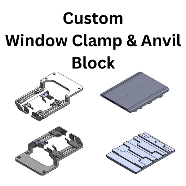
Custom Fabrication of Window Clamps & Anvil Blocks for the Semiconductor Industry

We provide custom fabrication of precision window clamps and anvil blocks designed to meet the high-accuracy, low-stress requirements of semiconductor manufacturing and inspection processes.

Our window clamps are engineered to securely hold delicate semiconductor components while maintaining a clear inspection or processing window, making them ideal for optical measurement, laser applications, metrology, and vision systems. The design ensures maximum stability without obstructing critical areas, enabling accurate, repeatable results.

Our anvil blocks are precision-machined to serve as stable reference and support surfaces for pressing, alignment, bonding, inspection, and measurement operations. Built for flatness, rigidity, and durability, they help maintain consistent part positioning and process reliability, even in high-volume environments.

Key Features & Benefits:

  • Custom-designed window clamps and anvil blocks based on part geometry and process requirements

  • Supports applications such as laser decapping, cross-sectioning, inspection, metrology, and automation

  • High-precision machining for tight tolerances and repeatable positioning

  • Minimizes stress, deformation, and vibration on sensitive semiconductor parts

  • Materials compatible with cleanroom, ESD-safe, and contamination-controlled environments

  • Improves measurement accuracy, process stability, and throughput

  • Suitable for R&D, pilot lines, and full production

From design validation to final fabrication, our window clamps and anvil blocks are built to protect critical components while enabling precise, unobstructed access for inspection and processing—because in semiconductor manufacturing, control, consistency, and microns matter. 🔬⚙️

If you want, I can also:

  • condense this into a one-paragraph website version

  • make a highly technical spec-style description

  • or tailor it for laser, metrology, or FA equipment applications

More Minor Products:

Model IT-5 IT-20
Units N.m, kgf.cm, ibf.in
Effective Range +/- 0.02 ~+/- 5.N.m +/- 2 ~ +/- 20N.m
Resolution 0.001N.m 0.01N.m
Accuracy +/- 0.5% of F.S
Maximum Allowable Torque 150%
Maximum Memory Data 511
Comparator Upper & Lower Limit Setting of Specification
A/D Convertor 16 Bit
Response 640Hz/sec
Battery Operated Ni.MH Battery with Power Adaptor
Operating Temperature 10~40 Deg C & Humidity of 85% & Below
Data Output RS232C Interface
Dimension W230 x H60 X D149mm
Mass Approximately 3.3kg

Radiographic Testing (RT) is a non-destructive testing (NDT) method which uses X-rays to examine the internal structure of manufactured components to identify any flaws or defects. Microfocus X-ray CT scanning is a 3D non-destructive testing (NDT) technique that allows the testing and 3D analysis of various materials in a non-destructive manner. It is widely used in the measurement of automotive parts, resin molded parts, bones, printed circuit boards (PCB), batteries, polymers, etc.

Shimadzu provides a comprehensive lineup of microfocus X-ray CT systems and solutions for high resolution 3D imaging of a wide variety of samples. Our product lineup includes the XSeeker 8000 bench-top X-ray computed tomography (CT) system, which enables clear observation of metal parts included in compact designs; and the inspeXio 7000 high-performance microfocus X-ray CT system, boasting higher resolution and higher contrast CT images with an intuitive user interface. Learn more about our full lineup below.

CHARACTERISTICS
  1. Easy operation
  2. Peak hold function
  3. Comparator function
  4. Memory function
  5. Automatic power off
  6. Local Newton value input

Radiographic Testing (RT) is a non-destructive testing (NDT) method which uses X-rays to examine the internal structure of manufactured components to identify any flaws or defects. Microfocus X-ray inspection is a 3D non-destructive inspection (NDI) technique that allows the testing and 3D analysis of various materials in a non-destructive manner. It is used in a wide range of industries, including the electronics, automotive, semiconductors, and aerospace industries.

Shimadzu provides a comprehensive lineup of microfocus X-ray inspection systems and solutions for high resolution inspection of electronic assemblies, components, and printed circuit boards (PCB). Our product lineup includes the Xslicer SMX-1010/1020, boasting significantly improved image quality and a simplified workflow; and the Xslicer SMX-6010, featuring high-accuracy images with a wide dynamic range that enables detailed observation of internal structures and defects. Learn more about our full lineup below.

In order for you to view this file we ask that you provide us with some information.