BOFA Fume Extraction & Filtration System

Description:

Market Leading Technology

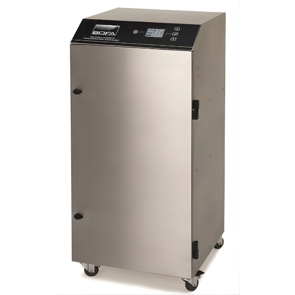
BOFA designs, develops and manufactures fume and dust extraction systems for a wide range of industrial sectors and applications. BOFA creates technologies that protect the health of millions of workers around the world while at the same time improving industrial process performance by minimising disruption to production.


These products ensure operator safety by capturing harmful dust and fumes which are generated during industrial processes while minimising disruption on production.

Why You Need Fume & Dust Extractor?

All businesses have a legal obligation to ensure a safe working environment for their people.


To maintain a dust and fume-free workplace through the removal of solid particles (particulates), liquid droplets (usually aerosols or mists) and vapours or gases (fume). This is critical, because the health consequences for employees working in a hazardous environment can be significant and permanent.


Work related lung illnesses (occupational respiratory disease) include asbestosis, silicosis, COPD, asthma, emphysema and lung cancer.

BOFA Fume Extractor
BOFA Fume Extractor

Award Winning Technology

BOFA was awarded the Queen’s Award for Enterprise 2017 for Innovation!

In 2017 BOFA was awarded the Queen’s Award for Enterprise: Innovation for our revolutionary Intelligent (iQ), Operating System , which is transforming the way that organisations around the world are able to protect the health of employees and improve production processes. Our Queen’s Award for International Trade in 2012, recognises that over 90% of our products are now exported overseas.

Find Suitable Fume Extractor System

Special for Your Industry

More Laser Application:

LAYER-BY-LAYER ABLATIONS

Decapsulation

Decapsulation (Decap) is a process that most Failure Analysis labs use on a routine basis.

The FALIT™ uses our patented laser technology to allow an operator to remove mold compound all the way through the lead frames to the substrate. The entire process is 100% controllable by the operator through our Graphic User Interface. The FALIT™ laser can accurately remove the entire compound, individual layers or sections of the mold compound (operator defined). The FALIT™ offers a safe and more accurate process for IC laser decapsulation.


Programmable Gas Assist comes standard to enhance the lasers capabilities while processing. Additional standard features include a camera system with external monitor cross hair generator, and process viewing for part alignment. An optional vision system can provide image recognition for part alignment or hole inspection.


Large Filler Mold Compounds for Copper

Our Digital ICO™ (IC Optimized) laser was specifically developed for removing the newer mold compounds associated with gold, copper, palladium, aluminum, and silver alloy bond wires. This compound typically has larger fillers and more filler material making it difficult even for traditional laser decapsulation. The greater laser power required to remove this new compound can sometimes damage very small wires or leave excess compound around the wires. Our new proprietary laser technology totally eliminates this problem and can even enhance results on traditional mold compounds.

Decapsulation Applications


The 532nm green laser within our FALIT ™ and the FALIT Duo™ offers FA labs a longer depth of focus for cross-sectioning thicker parts with the draw-back of having a larger spot size and larger Heat Affected Zone (HAZ) than the UV laser. The green laser has been employed by many semiconductor failure analysis labs for cutting parts out of PCBs where the solder balls, and surrounding components, cannot be damaged. The green laser is also used for cutting electronic components in half as a pre-process to either Focused Ion Beam (FIB) cross-sectioning, or mechanical polishing. Our experience shows that we can get to within about 75-microns from the area of interest without damaging it while using the green laser. As, in most cases, our process for preparing a sample for solder ball adhesion inspection does not melt the solder ball, the FA lab is able to quickly process a sample to further analyze the solder-to-pad adhesion without introduction of external force or heat which might otherwise call into question the inspection results.

With the optional 355nm UV laser within our FALIT ™ and the FALIT Duo™ offers higher precision, a smaller spot size, and a smaller Heat Affected Zone over the green laser. The UV laser is recommended where the failure analysis lab processes, via cross-sectioning or cutting, a wider array of different packages, or when dealing with silicon wafers. Cuts from the UV laser are much more fine which allows more bulk material to be removed in an effort to get closer to the area of interest during cross-sectioning. Silicon wafers can be sliced and diced with up to 10-watts of UV power. As UV is absorbed by most materials, it provides the FA lab with the flexibility to process a wider array of parts.

LASER TYPE AND HEAT AFFECTED ZONE (HAZ) on Unfired ceramic
SCRIBE – DeLid – X Sectioning
Application Gallery

X Sectioning Gallery

Diamond saws and other mechanical methods of cross-sectioning put physical stress into a part. It is then difficult to determine whether the defect (such as delamination) was already there or caused by the mechanical process itself. Laser cutting presents NO such problem. There is no mechanical force introduced with a laser. Therefore, cross-sections can be made much closer to the actual defect diminishing the polishing time or in many cases eliminating polishing altogether

SCRIBE – DeLid Gallery

Lids and covers over components that need to be analyzed have always been a problem in the Failure Analysis Lab. Mechanical micro routers can damage internal parts, require complicated fixtures, and even destroy samples. With the FALIT™ Laser this process is quick, simple, and successful. A Green laser (532nm), or a UV laser (355nm), can be used to cut the top of a lid completely off.

The FA Cube™ was specifically designed with the semiconductor failure analysis and forensics Labs in mind. Our compact laser semiconductor laser decapsulation system provides clean and accurate laser IC Laser Decapsulation with reliable results. The FA Cube™ incorporates the same patented process as our FALIT™ series. This patented laser process uses multiple laser configurations to provide clear and precise test samples for nearly every type of semiconductor failure analysis and forensic application.

  • Ideal Solution for IC Laser Decapsulation and removing large filler mold compounds for copper.
  • Cleanly remove mold compound using laser technology rather than the traditional unsafe acid process.
  • Expose Wire Bonds without damage to other components.
  • Fixed Co-Axial Optical Camera Lens (options available).
  • Optional X-Y stage table and Self-Centering Fixture.
  • Easy sliding door with large viewing window and internal workspace.
  • Compact Motorized Z-Axis for accuracy (optional).
  • FALIT™ Light Laser Software interface included. Basic GUI for Failure Analysis.


Software

Our essential FA Cube intuitive software allows the laser decapsulation of IC components for bond and die inspection. Aside from the standard software features, we offer a variety of modules and tools to extend the abilities of the machine per request.


Optional Software Tools:

  • Gasket Module
  • Polygon tools/Ortho Mode
  • Surround Mode
  • Text Mode
  • Image Import
  • Template Creation
  • Recipe Manager

IC Silicone Gel Compound Removal

A growing number of IC design are utilizing a gel type encapsulation  compounds.

Whether it is for diaphragm on the die of a pressure detection device. Less stress on the newer thinner dies, or extreme temperature variation and vibrations faced by automotive industry control semiconductor devices, this silicone gels seems impervious to chemical, plasma or even standard laser decapsulation..

Most power and MEM devices are silicone encapsulated.


A Case Note.

The SIFEL® gel from SHIN-ETSU is a remarkable material used in many semiconductors. Common devices using SIFEL® gel are MEMS devices and pressure sensors where low-stress encapsulation of sensitive electronic devices, but maximum protection against heat and chemicals, is important. SIFEL®’s advantages present unique challenges to failure analysis labs that need to remove the gel in order to determine why a device failed. With it’s near-impervious chemical resistance, acids and many other chemicals have no effect on the gel.


CLC has developed a laser application that uses SIFEL® gel properties to the advantage removing it


Using our proprietary ICO laser, and a carefully engineered removal recipe, the majority of the gel can be removed without too much problem.


CLC FALiT Gel Decapsulation Safely Removes Gel Compound “ALL THE WAT TO THE DIE” in second’s.

UNIQUES SILICONE GEL COMPOUND REMOVAL LASER TECHNIQUE
FALIT Gel
In order for you to view this file we ask that you provide us with some information.