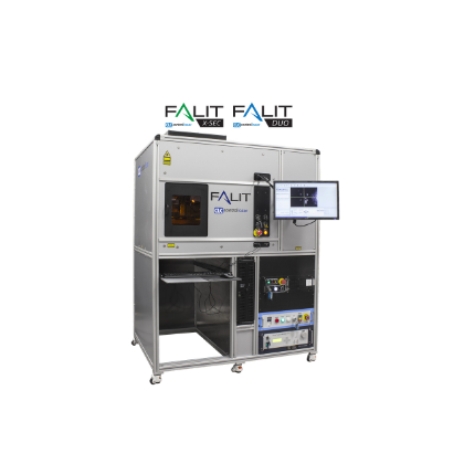
Laser Semiconductor Failure Analysis System
The FALIT™ incorporates a patented laser etching process with multiple laser configurations and wavelengths to provide clear and precise test samples for every type of semiconductor failure analysis application. The FALIT™ allows a faster and more accurate method for Failure Analysis semiconductor processing. Our patented semiconductor decapsulation etching technology provides clean, accurate laser IC Decapsulation, and more.
- Ideal Solution for IC Decapsulation, Gel Removal, Cross-Sectioning, and Delidding Components.
- Cleanly remove mold compound using laser technology rather than the traditional unsafe Acid process.
- Expose Wire Bonds without Damage to other components.
- Air-cooled (except for the optional UV laser).
- Integrated safety shutter to avoid potential beam exposure.
- FALIT™ Laser Software interface included. Fully featured, GUI for Failure Analysis.
The FALIT™ systems provide Decapsulation (etching) and Cross-sectioning of semiconductors for failure analysis labs. CLC IC laser etching systems are used in many semiconductor failure analysis labs to remove mold compound, de-lid semiconductor hermetically-sealed cases, remove various gels, and cross-section ICs for further inspection. Our patented process has been refined over the 10-plus years since it’s existence.


